
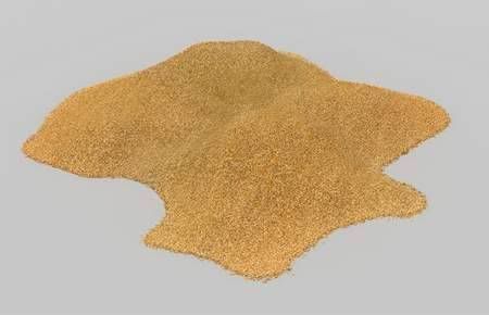
Sand. Made up of 25 percent silicon, is, after oxygen,
the second most abundant chemical element that's in the
earth's crust. Sand, especially quartz, has high percentages
of silicon in the form of silicon dioxide (SiO2) and is
the base ingredient for semiconductor manufacturing.
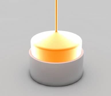
After procuring raw sand and separating the silicon,
the excess material is disposed of and the silicon is
purified in multiple steps to finally reach semiconductor
manufacturing quality which is called electronic grade
silicon. The resulting purity is so great that electronic
grade silicon may only have one alien atom for every one
billion silicon atoms. After the purification process,
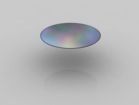
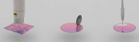
the silicon enters the melting phase. In this picture
you can see how one big crystal is grown from the
purified silicon melt. The resulting mono-crystal
is called an ingot.
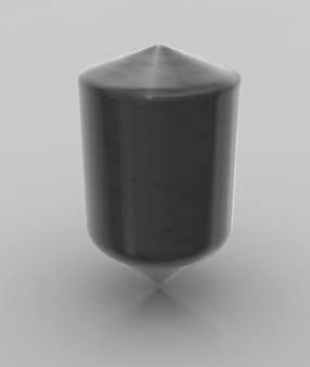
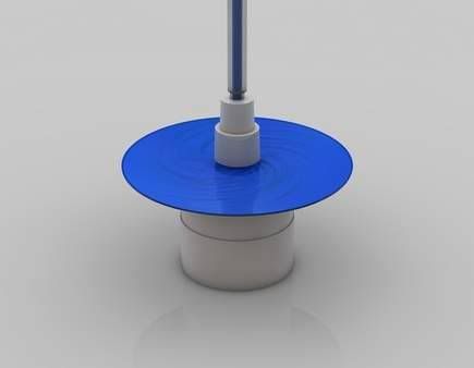
A mono-crystal ingot is produced from electronic grade
silicon. One ingot weighs approximately 100 kilograms
(or 220 pounds)and has a silicon purity of 99.9999 percent.
The ingot is then moved onto the slicing phase where
individual silicon discs, called wafers, are sliced thin.
Some ingots can stand higher than five feet. Several
different diameters of ingots exist depending on the
required wafer size. Today, CPUs are commonly made
on 300 mm wafers.
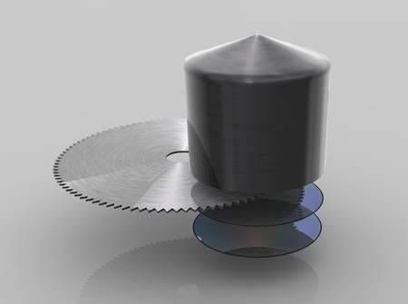
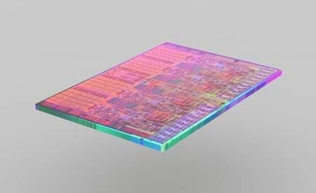
Once cut, the wafers are polished until they have flawless,
mirror-smooth surfaces. Intel doesn't produce its own ingots
and wafers, and instead purchases manufacturing-ready
wafers from third-party companies. Intel’s advanced
45 nm High-K/Metal Gate process uses wafers with a
diameter of 300 mm (or 12-inches). When Intel first
began making chips, it printed circuits on
50 mm (2-inches) wafers. These days, Intel uses 300 mm wafers,
resulting in decreased costs per chip.
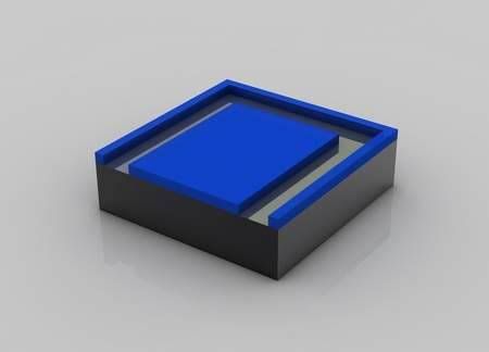
The blue liquid, depicted above, is a photo resist finish similar
to those used in film for photography. The wafer spins during
this step to allow an evenly-distributed coating that's smooth
and also very thin.
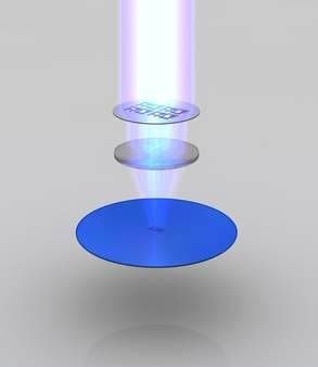
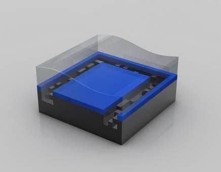
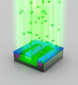
At this stage, the photo-resistant finish is exposed to ultra
violet (UV) light. The chemical reaction triggered by the UV
light is similar to what happens to film material in a camera
the moment you press the shutter button.
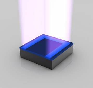
Areas of the resist on the wafer that have been exposed to UV
light will become soluble. The exposure is done using masks
that act like stencils. When used with UV light, masks create
the various circuit patterns. The building of a CPU essentially
repeats this process over and over until multiple layers are
stacked on top of each other.
A lens (middle) reduces the mask's image to a small focal point.
The resulting "print" on the wafer is typically four times smaller,
linearly, than the mask's pattern.
In the picture we have a representation of what a single
transistor would appear like if we could see it with the naked eye.
A transistor acts as a switch, controlling the flow of electrical
current in a computer chip. Intel researchers have developed
transistors so small that they claim roughly 30 million of
them could fit on the head of a pin.
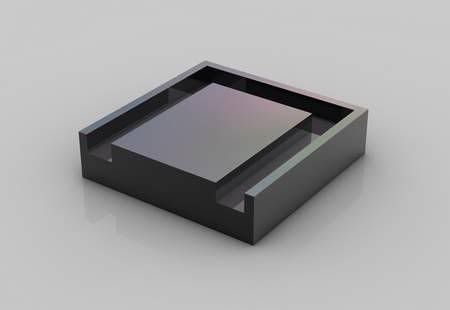
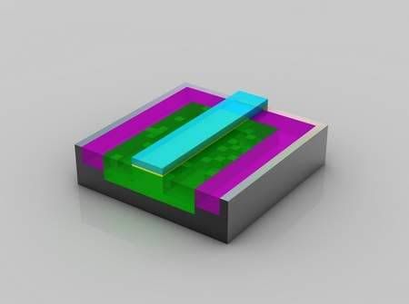
After being exposed to UV light, the exposed blue photo resist
areas are completely dissolved by a solvent. This reveals a
pattern of photo resist made by the mask. The beginnings of
transistors, interconnects, and other electrical contacts
begin to grow from this point.
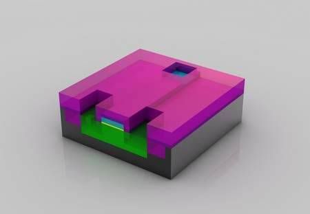
The photo resist layer protects wafer material that should
not be etched away. Areas that were exposed will be etched
away with chemicals.
After the etching, the photo resist is removed and the
desired shape becomes visible.
More photo resist (blue) is applied and then re-exposed to
UV light. Exposed photo resist is then washed off again
before the next step, which is called ion doping.
This is the step where ion particles are exposed to the wafer,
allowing the silicon to change its chemical properties in
a way that allows the CPU to control the flow of electricity.
Through a process called ion implantation (one form of a process
called doping) the exposed areas of the silicon wafer are
bombarded with ions. Ions are implanted in the silicon wafer
to alter the way silicon in these areas conduct electricity.
Ions are propelled onto the surface of the wafer at
very high velocities. An electrical field accelerates
the ions to a speed of over 300,000 km/hour(roughly 185,000 mph)
After the ion implantation, the photo resist will be removed
and the material that should have been doped (green) now has
alien atoms implanted.
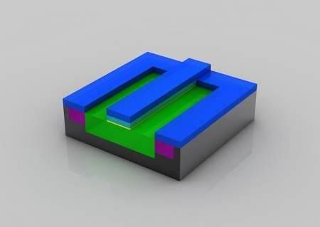
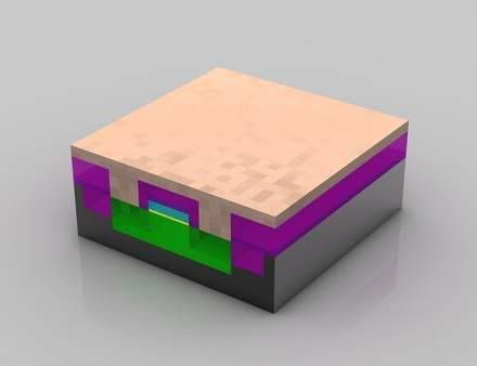
This transistor is close to being finished. Three holes have
been etched into the insulation layer (magenta color) above
the transistor. These three holes will be filled with copper,
which will make up the connections to other transistors.
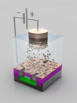
The wafers are put into a copper sulphate solution at this stage.
Copper ions are deposited onto the transistor through a process
called electroplating. The copper ions travel from the positive
terminal (anode) to the negative terminal (cathode)
which is represented by the wafer.
The copper ions settle as a thin layer on the wafer surface.
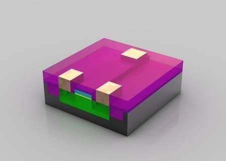
The excess material is polished off leaving
a very thin layer of copper.
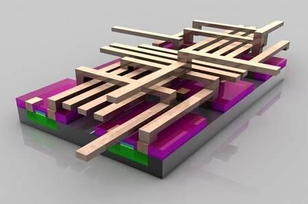
Multiple metal layers are created to interconnects (think wires)
in between the various transistors. How these connections have
to be “wired” is determined by the architecture and design
teams that develop the functionality of the respective processor
(for example, Intel’s Core i7 processor). While computer chips
look extremely flat, they may actually have over 20 layers to
form complex circuitry. If you look at a magnified view of a chip,
you will see an intricate network of circuit lines and
transistors that look like a futuristic, multi-layered
highway system.
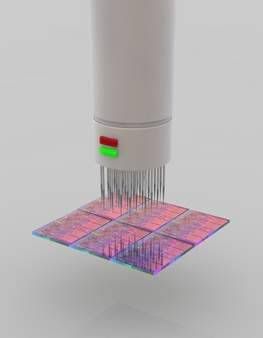
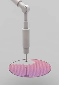
This fraction of a ready wafer is being put through a first
functionality test. In this stage test patterns are fed into
every single chip and the response from the chip monitored
and compared to "the right answer."
After tests determine that the wafer has a good yield of
functioning processor units, the wafer is cut into pieces
(called dies).
The dies that responded with the right answer to the test
pattern will be put forward for the next step (packaging).
Bad dies are discarded. Several years ago,
Intel made key chains out of bad CPU dies.
This is an individual die, which has been cut out in the
previous step (slicing). The die shown here is a die of
an Intel Core i7 processor.
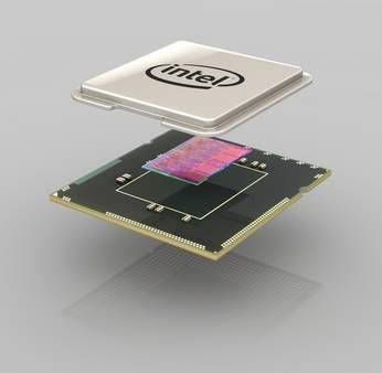
The substrate, the die, and the heatspreader are put
together to form a completed processor. The green
substrate builds the electrical and mechanical interface
for the processor to interact with the rest of the PC
system. The silver heatspreader is a thermal interface
where a cooling solution will be applied.
This will keep the processor cool during operation.
A microprocessor is the most complex manufactured product
on earth. In fact, it takes hundreds of steps and only
the most important ones have been visualized in this
picture story.
During this final test the processors will be tested for
their key characteristics (among the tested characteristics
are power dissipation and maximum frequency).
Based on the test result of class testing processors with
the same capabilities are put into the same transporting trays.
This process is called "binning". Binning determines the maximum
operating frequency of a processor, and batches are divided
and sold according to stable specifications.


0 comments:
Post a Comment